Figure 1. Schematic of PDMS stencil fabrication and micropatterning. A: Microfabricated photoresist pillars on a silicon wafer. B: Polydimethylsiloxane (PDMS) prepolymer spun on a silicon wafer with photoresist patterns. C: Peeling the cured PDMS stencil off the silicon wafer. D: Illustration of cell seeding on the stenciled coverslips. E: Representative schematic of the formation of the RPE monolayer. F: Characteristic circular pattern of the RPE cells after the PDMS stencil is peeled off the coverslip.
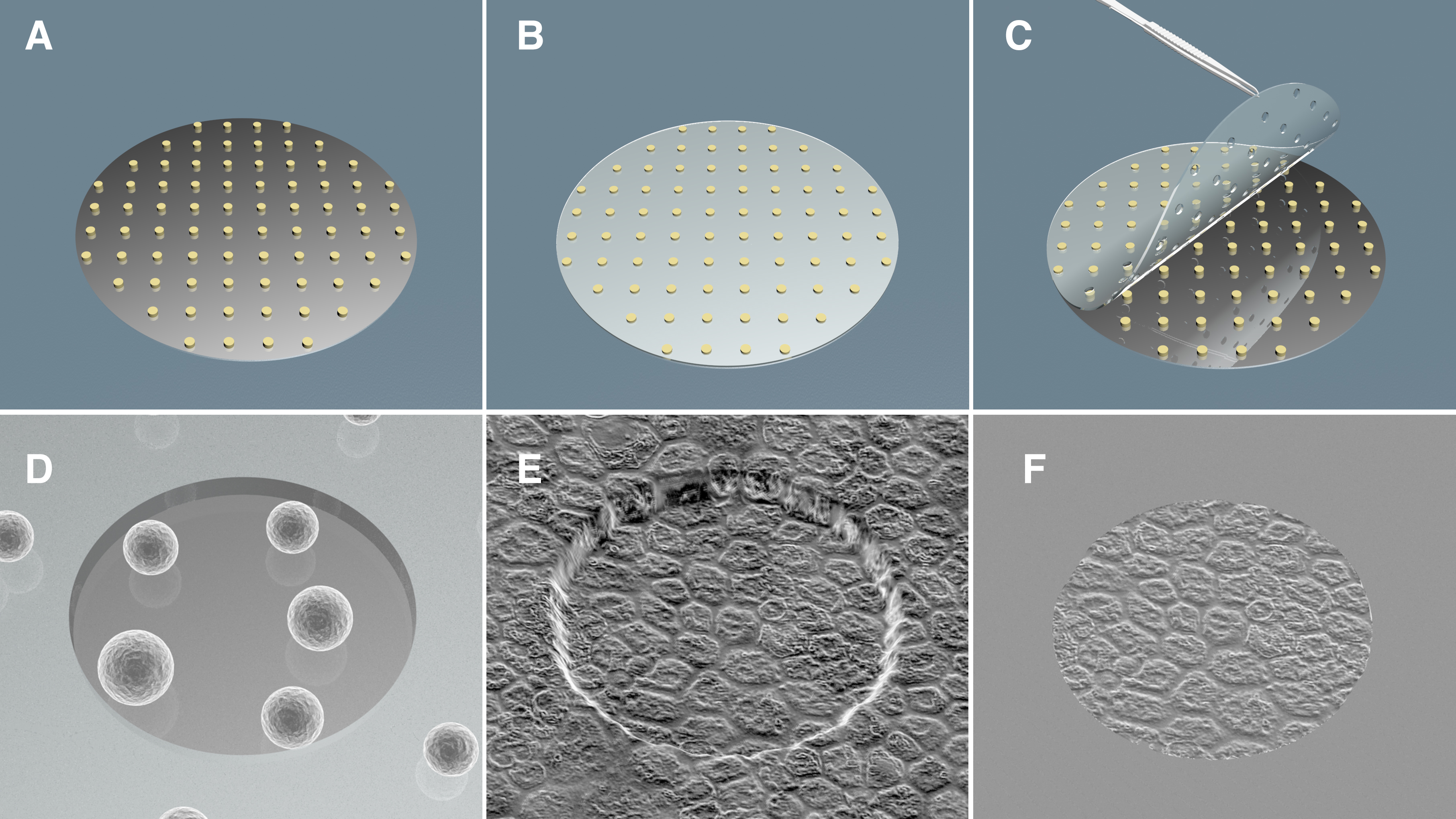
 Figure 1 of
Farjood, Mol Vis 2017; 23:431-446.
Figure 1 of
Farjood, Mol Vis 2017; 23:431-446.